
When microchips are faulty, it’s the job of the Dresden-based experts at SGS Institut Fresenius to find out why.
Electrostatic discharge (ESD) is one of those things we’ve all experienced in our everyday lives. You go to touch something, and suddenly a spark flies. This is caused when the difference of electrical potential between the two bodies is large enough to lead to a charge equalisation. These kinds of electrostatic discharge involve comparatively low amounts of energy, but they are sufficient to cause critical damage to certain circuit elements in microchips. Although there are protective circuits, they have limited effectiveness. This is why rigorous ESD tests are conducted on components ahead of market launch to discover potential weak points. However, ESD damage frequently occurs when end customers use the component, at which point it is returned to the supplier, who then attempts to determine the cause of the potential ESD damage. In both cases, this is where the Dresden site of SGS Institut Fresenius GmbH, which focuses on microelectronics and is a leading service provider for analysis in this field, comes in.
The ESD damage is in the detail
Mechanical engineering has primarily provided workstation solutions that ensure effective ESD protection. These include special clothing, floor surfaces, table tops and frames, for example. However, an electron microscope is required to determine fine ESD damage after the event. “Only rough damage with significant fusing would be visible under an optical microscope, but that is not generally the case, as ESD damage causes relatively little fusing. The first step is removing the entire wiring level of a damaged component in a wet-chemical process – that is to say, by etching it away with acid,” laboratory manager Thomas Freitag explains. This makes the actual semiconductor level – and thus also the silicon substrate – visible. The transistors are located on this level, along with all those components that are susceptible to ESD.
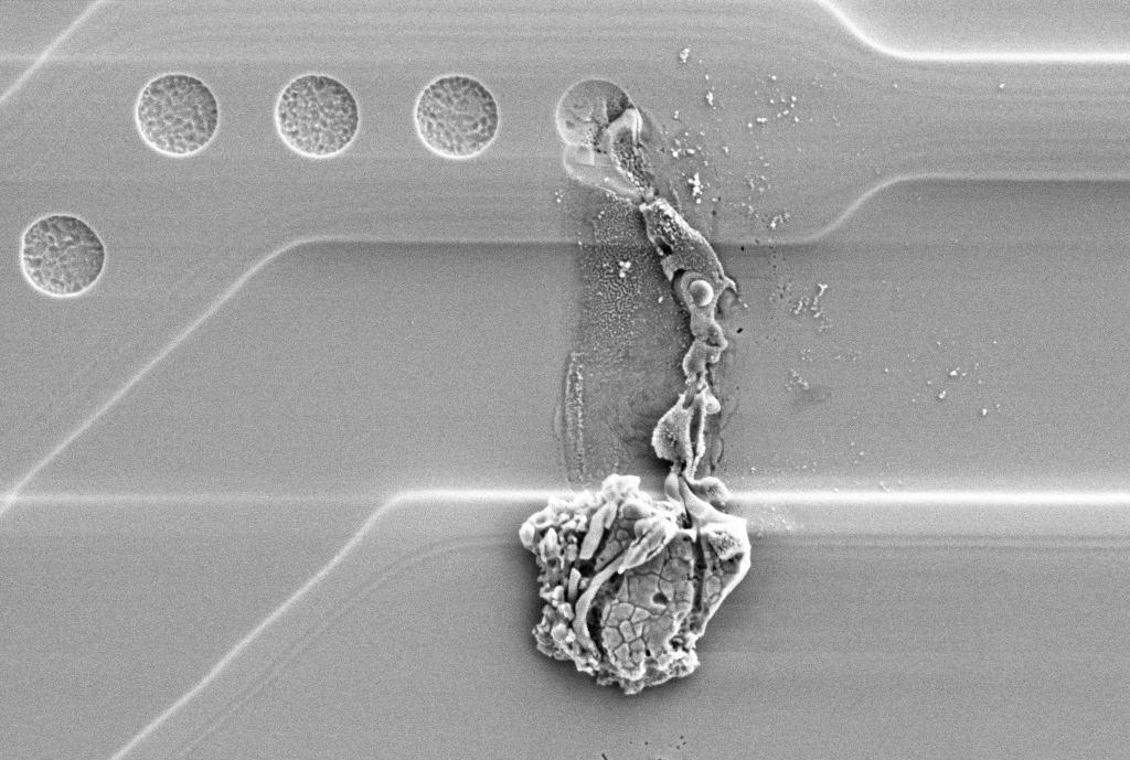
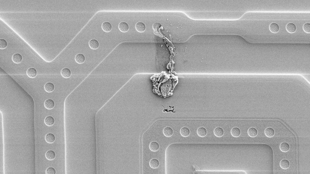
The discharge generates flash temperatures of well over 1000 degrees, causing the silicon surface to melt.
With the help of electron microscope analysis, it is possible to trace the flashover current path on these components, which is created by an electrostatic discharge. “The discharge generates flash temperatures of well over 1000 degrees, causing the silicon surface to melt,” site manager Gerald Dallmann says. This kind of flashover current path is located between two active areas (appear raised on figures 1 and 2). In such cases, ESD damage is clearly identifiable, as it is very characteristic.
Identifying ESD damage – only one part of the service portfolio
However, there are also jobs where testing equipment is used to deliberately load components. This kind of ESD test is helpful e.g. for newly developed circuits in preparation for market launch. “The following questions are relevant in tests where a charge is used to load or overload the components: Where exactly did the damage occur? Which protective circuits were effective and which weren’t?” says Dallmann. ESD simulation models are used to ensure the components are loaded realistically. The most common models include the human-body model (HBM) and the machine model (MM). While an HBM simulates the discharge from a human body into a component, the MM simulates discharge from a machine.
The energies involved in EOS are much larger, and can cause a component to melt right through.
In addition, it is often necessary to decide whether it involves ESD or even EOS (“electrical overstress”). This isn’t always easy. Fundamentally, electrical components are always dimensioned and constructed for specific maximum currents and voltages. “When the component is overloaded, however, this causes flashovers that differ greatly from those associated with ESD. The energies involved in EOS are much larger, and can cause a component to melt right through,” Dallmann explains. EOS generally arises when the customer is using the component. However, there are also cases where it becomes hard to differentiate between ESD and EOS, so every nuance matters.
Global network of experts
SGS Institut Fresenius GmbH is a key provider of non-medical analytics. The independent laboratory was originally founded in Wiesbaden in 1848. In 2004, it became part of SGS, the world’s leading testing and certification company. This Swiss testing Group has a global workforce of over 97,000, spread across more than 2,600 sites. Every site has its own specialism. The fact that the Dresden site focuses on ESD is largely due to its long tradition of microelectronics. Two departments of what was then the Zentrum Mikroelektronik Dresden formed an independent company in 1990. They are now one of the leading industrial service providers for characterising materials, surfaces and thin layers. Alongside the actual analysis, their expertise and wide-ranging network enable Gerald Dallman and his team to provide companies with targeted support.
Do you want to keep up to date on the various ways that item solutions are being put to use? Then we have the perfect solution for you. Simply subscribe to the item blog by completing the box at the top right!